Semiconductor Measurements and Inspection
Measurement
Thin film thickness measurement system SE,SR
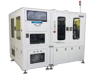
■ Model : AS-TEO, AS-TRC
● Application field : Wafer, Display, Thin Film, Sample Analysis, Biosensor, Solar Thin Film, Drug Coating, etc.
● Measurement item : Thickness measurement of single and multilayer thin films in the range Å ~ ㎛


| Model : AS-TEO, AS-TRC |
Beam Diameter | 120㎛ *300㎛ | ||
|---|---|---|---|---|
| Spectral Range | 245m to 1000m (Option:~ 1700nm) | |||
| UV Spectrometer | 1.6nm pixel resolution, ~5nm | |||
| NIR Spectrometer | 3.2m pixel resolution, ~10m bandwidth (NIR) | |||
| Options | Can be linked to internal processes and instruments by linking SPC and MES | |||
| Fast Camera Sample Alignment | ||||
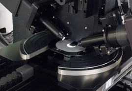
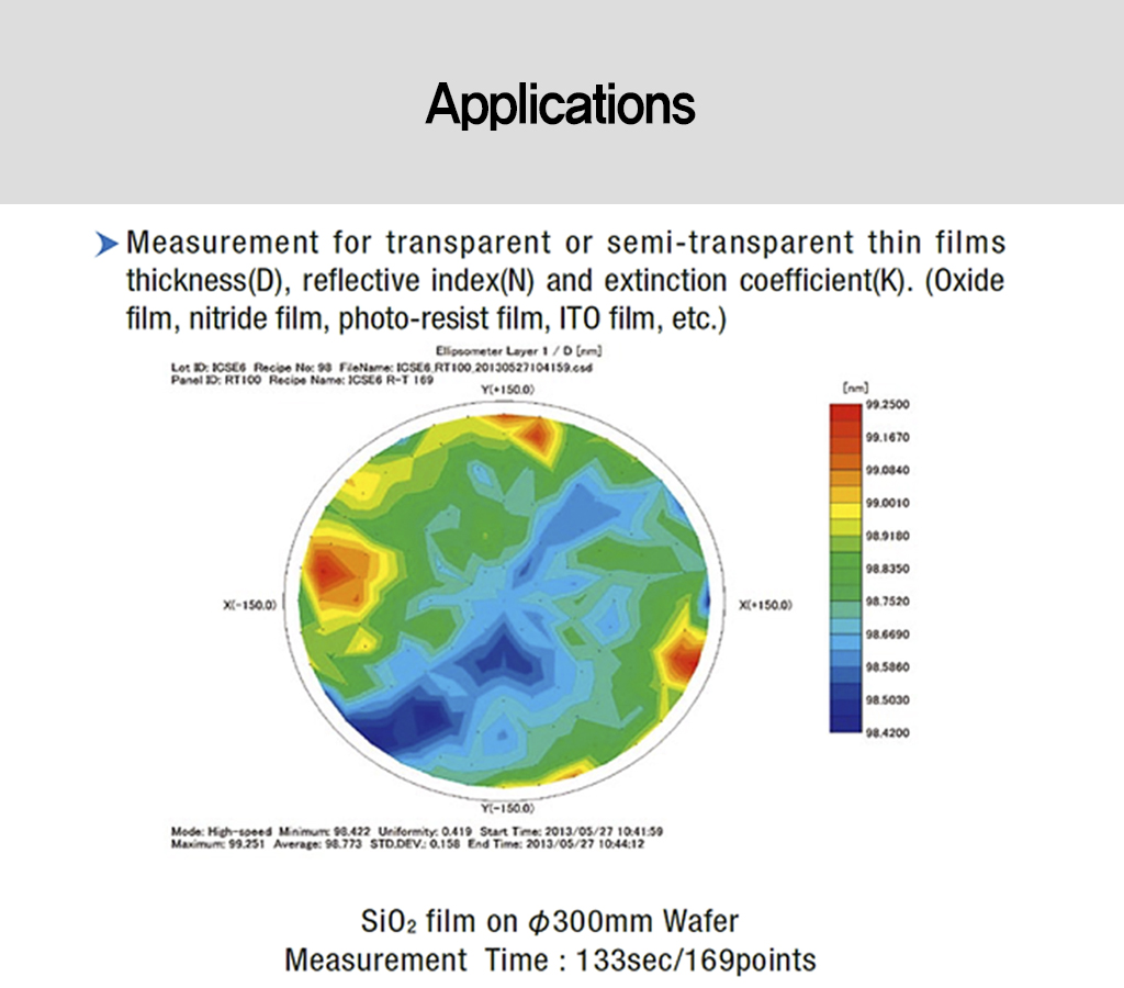
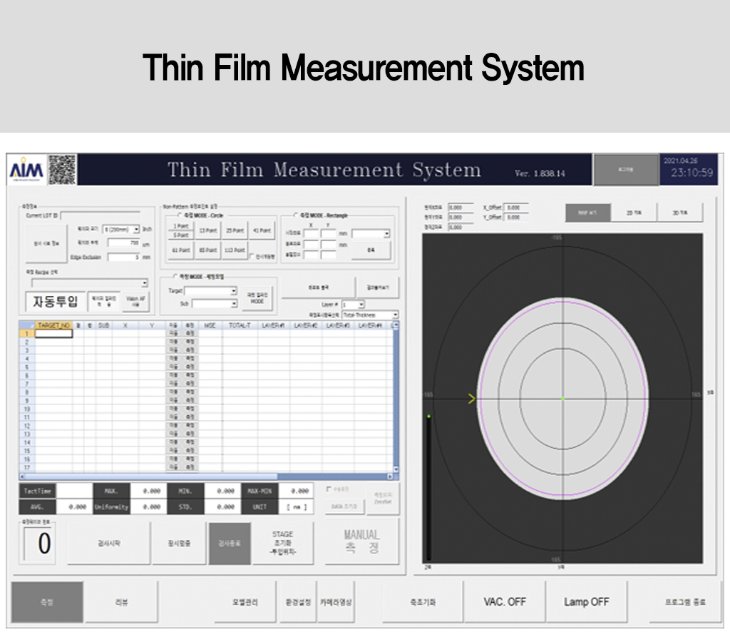
■ Full Auto Mapping Thin-Film Measurement System (Ellipsometer or Reflectometer)
Measurement
Metal Thin Film Measurement System
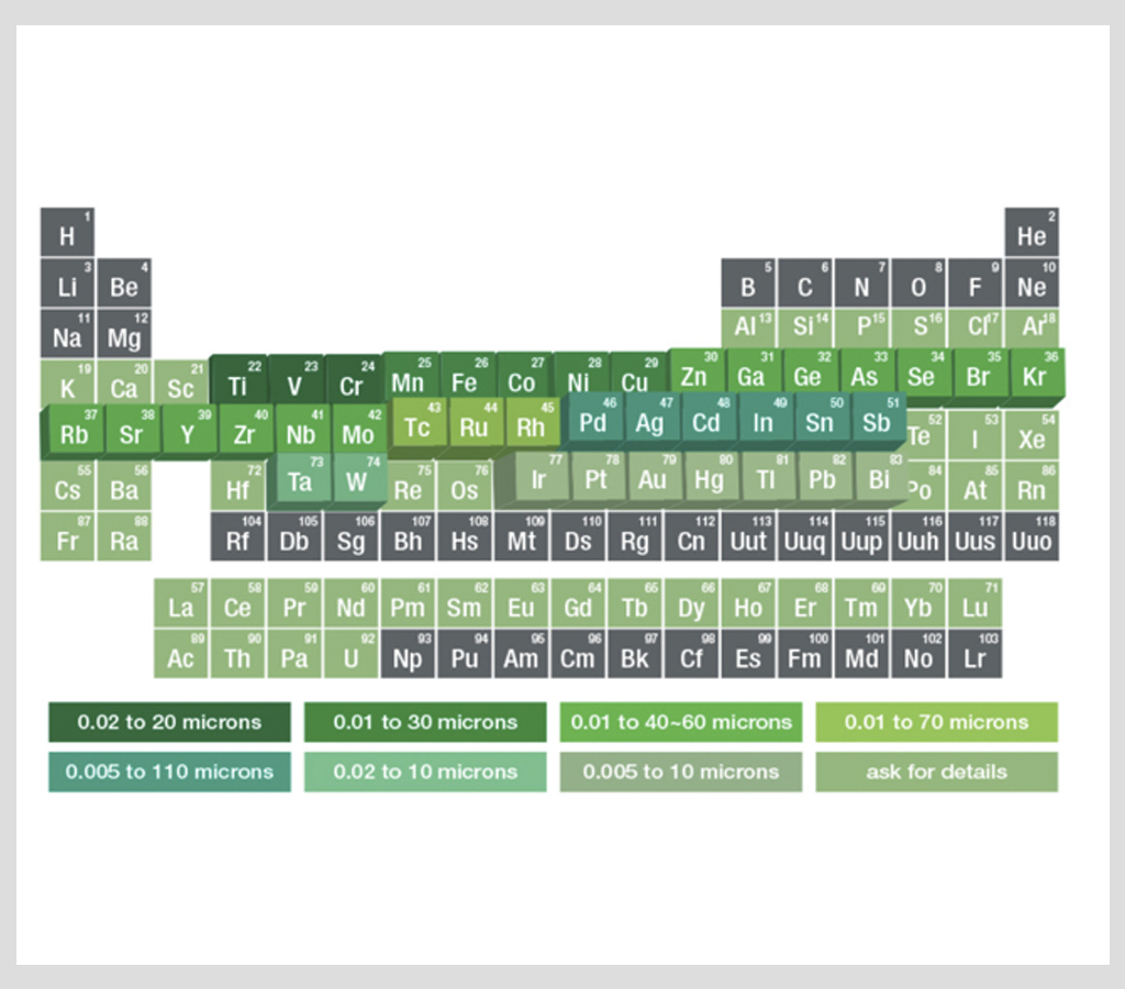
■ Micro XRF System

■ Model : AX – 128
● Measurement target: Metal thin film, plating, coating thickness measurement, material composition ratio measurement
● Measurement items: A total of 5 layers including materials (10 elements in each layer), simultaneous measurement of 25 elements
| Model: AS-TXR | wafer size | 4~12inch | ||
|---|---|---|---|---|
| X-ray | 50W Mo target with Capillary Optics | |||
| Beam spot size | 7.5㎛ FWHM | |||
| detector | Larger Window, 70mm2, high flux SDD with 135eV resolution | |||
| focus distance | ~ 0.5 mm (0.02inch) | |||
| Video magnification | 매크로 – 45x (5x digital zoom) | |||
| Micro- 150× | ||||
| Option | Interworking with SPC and MES to interlock with internal processes and instruments | |||
| Application field | Wafer, Display, Thin Film, Bump, RoHs, Heavy Metal Analysis, Component Analysis, Impurity Content Analysis, Food Trace Element Analysis, Dental Material Analysis, Battery Electrode Material Analysis etc. | |||


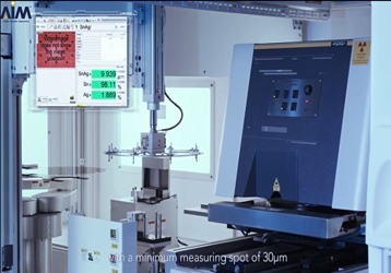
■ Micro XRF System
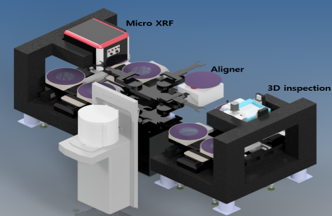
Semiconductor
Semiconductor-Wafer surface inspection
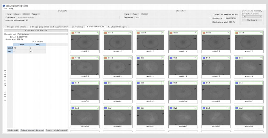
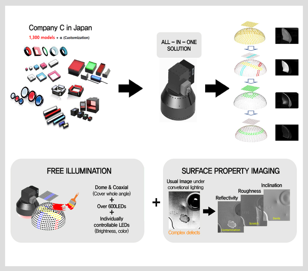
■ Deep Learning - Wafer inspection System
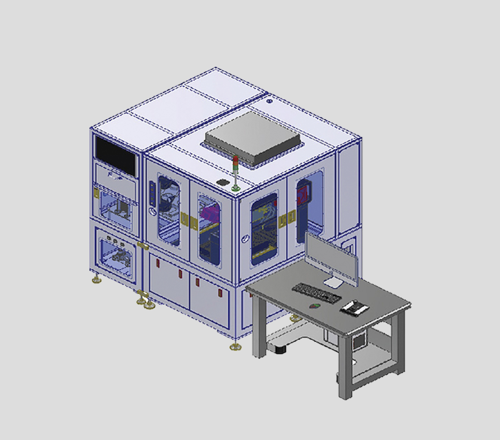
– Best abrasive, stain detection using 360-degree multi-lighting and image processing technology
Result (optical filter treatment only)

Result (optical filter treatment only)

After_Processing
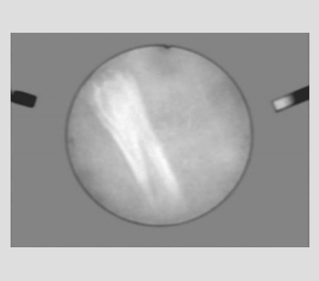
After_Processing
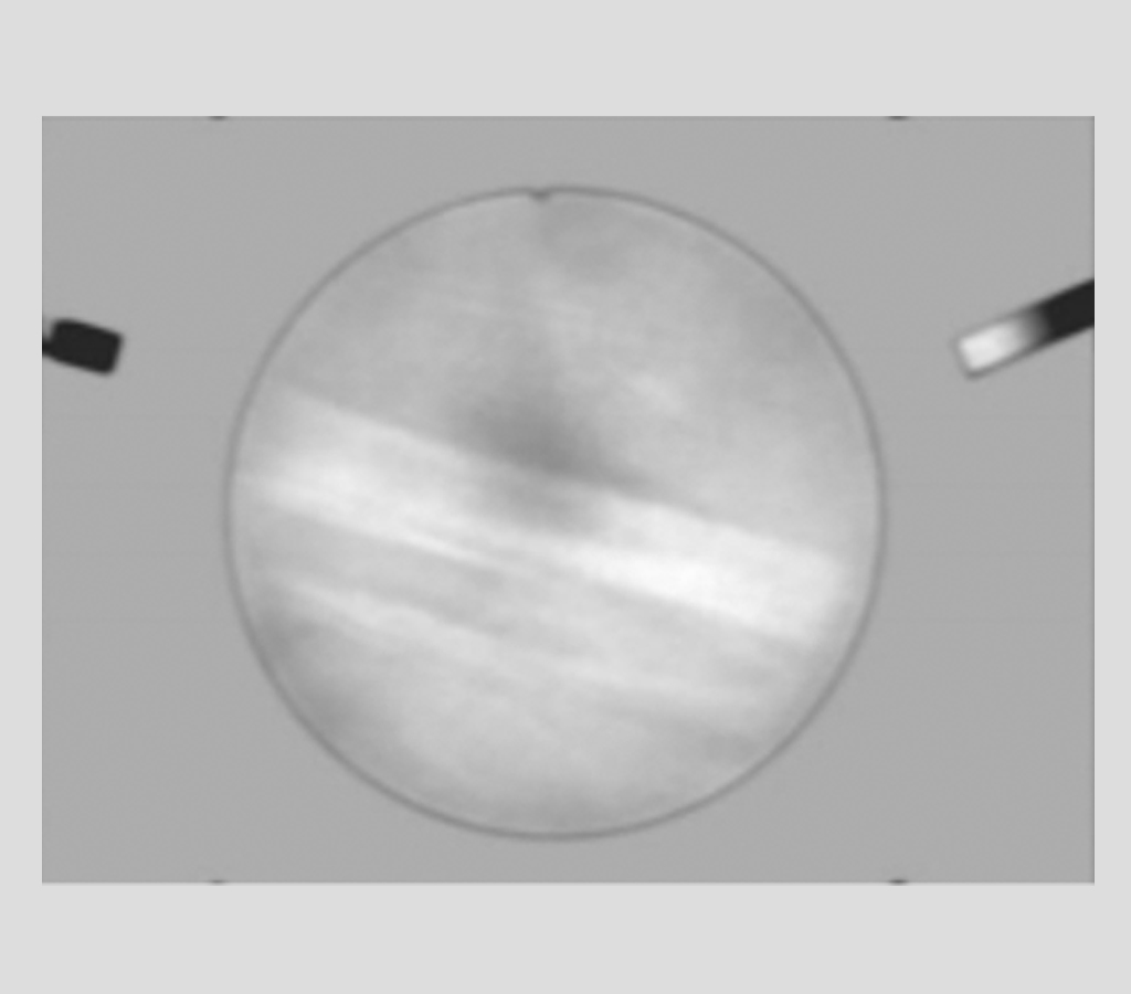
– 360 degrees Free illumination & Surface Property imaging
Just one sensor can do the inspections impossible so far
Semiconductor
Semiconductor-Wafer measurement
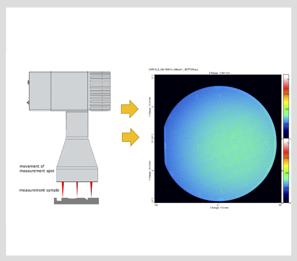
■ Monitoring wafer Bow, Warp, TTV and Thickness measurement
■ Characteristics
Balwafer Bow, Warp, TTV (total thickness variation), and thickness measurements are important factors in evaluating wafer flatness and uniformity in semiconductor manufacturing. The meanings of each item are as follows.
Bow: This is a measure of the degree of curvature from the center of the wafer to the edge. It indicates how bent the wafer is, and in a process where flatness is important, the lower the Bow value is, the better.
Warp: represents the extent to which the wafer is twisted, similar to the bow, but measures the bending across the wafer. It is used to evaluate the overall geometric flatness of the wafer.
Total Thickness Variation (TTV): Indicates the difference in thickness between the thinnest and thickest parts of the wafer. TTV is an important indicator for processes that require uniform thickness of the wafer.
Thickness measurement: Evaluate uniformity and accuracy by measuring the average thickness of a wafer.
This measurement monitoring is essential to maintain the quality of the semiconductor manufacturing process and to reduce defects in subsequent processes. The Bow, Warp, TTV, and thickness values must be appropriate so that the wafer can be processed without problems in subsequent processes.
EFFICIENT
- elegance
- swift
- non-contact
VERSATILE
- High-speed area inspection for offline and inline quality control
- Simple POI inspection with definable scan shapes and filters
- Centrifugal imaging for best results on reflective surfaces
USER-FRIENDLY & SAFE
- 간편한 통합
- 비파괴 측정
- 견고함
- 파일럿 레이저
■ 3 TECHNICAL SPECFICATIONS OF FLYING SPOT SCANNER

■ Specification
| SPEC | Field of view [mm] | 310 | 80 | 40 |
|---|---|---|---|---|
| Acceptance angle [°] | ± 0.5 | ± 1 | ± 2.5 | |
| Working distance [mm] | 150 | 200 | 122 | |
| Lateral Resolution [㎛] | 30 | 20 | 6.5 | |
| Dimensions (h x I x w )[mm] | 700 × 370 × 370 | 288 × 114 × 201 | 235 × 101 x 201 | |
| Weight | 29 Kg | |||
| Suited CHR controller | CHR 2IT DW | CHR 2IT, 2IT DW, 2LR | CHR 2IT, 2IT DW | |
| Availability | Beg. 2023 | Fully available | Fully available |
Semiconductor
Semiconductor-Wafer thickness measurement
■ NCG thickness meter
Summary
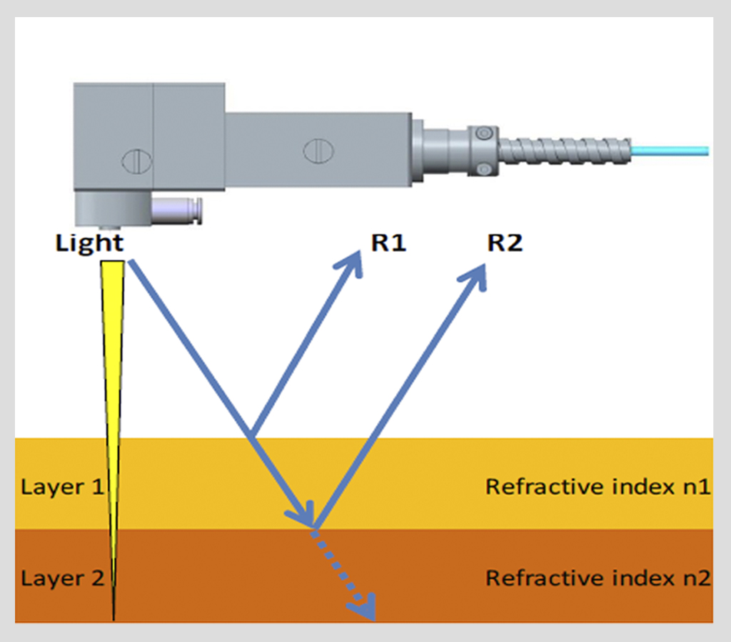
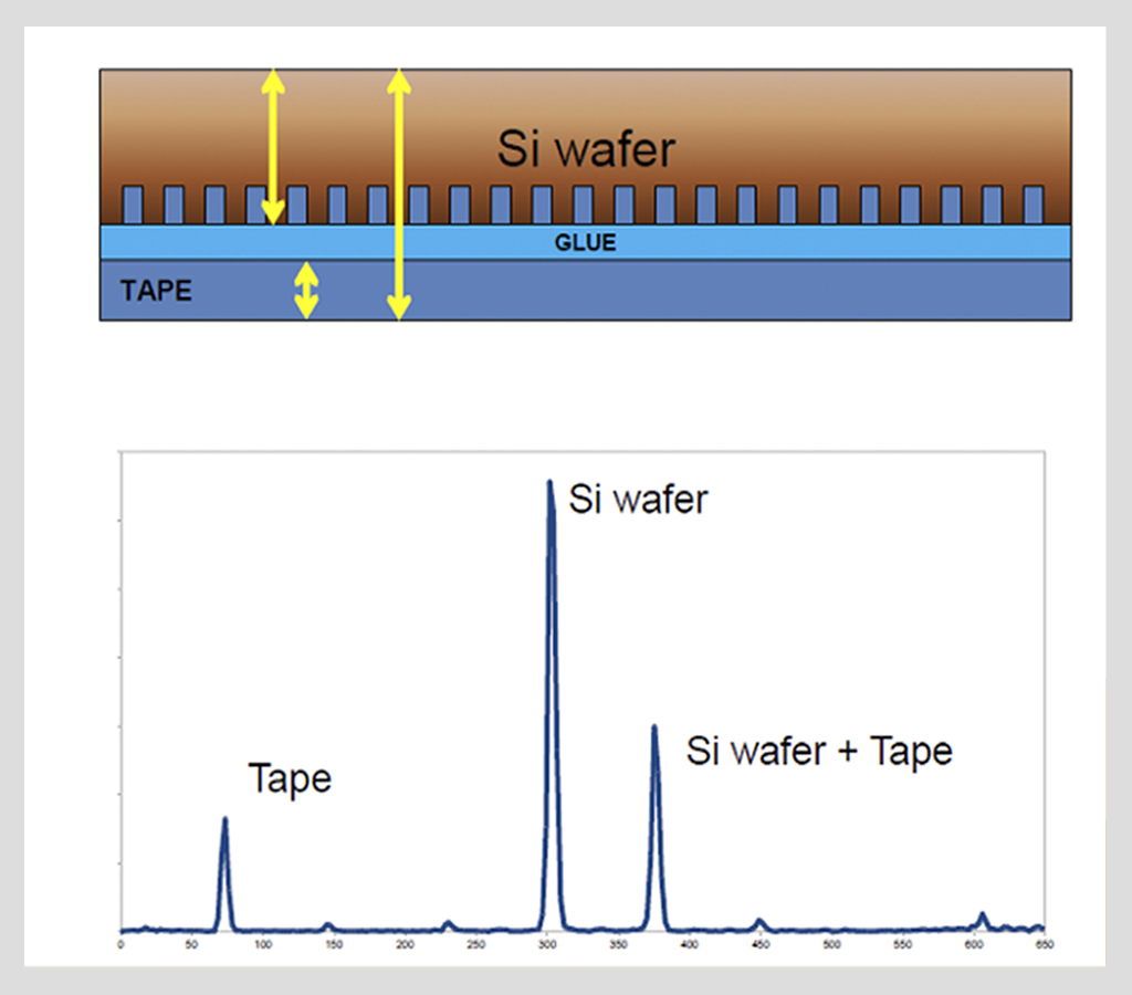
NCG is a thickness meter based on interferometry technology.
The constant light waves reflected from the layer are separated at the boundary of the object to be measured and measure the thickness of each layer.
NCG is designed to control the thickness of different types of parts such as glass, plastic, and silicon wafers.
Infrared light sources can be used to measure opaque materials. Our gauges show the mechanical cycle time,
Designed to improve and maintain the quality of the final product and to control the process before, during, or after the main stage of work.
NCG is a high-speed precision meter that can interface with any machine for accurate and fast part thickness control.
Within the specified technical specification limits, it can be installed and used inside the fixture or machine, regardless of dry or humid conditions.
Applications
• Various types of silicon. Sapphire wafer thickness measurements
• During process control of background grinding machines and wrapping machines
• Measure each thin or thick layer
• Tape thickness control
advantage
• Ensure part production within target tolerance
• Measurement time optimization
• Guaranteed uniform productivity control
• guaranteed production improvement
• Production history tracking
Measurement Principle | Interferometric |
light source | SLED |
Model-specific measurement range* | S1 =37~1850㎛ S2 = 74~3700 ㎛ T1 = 15~900 ㎛ D2 = 60~3000 ㎛ |
Accuracy | ≤ 1㎛ |
axial resolution | 30 nm |
Number of applied channels | 1 |
Interface | Ethernet (10/100 Mbit) RS232 / RS422 as option |
Network Connection | available |
Supply power | 12 ÷ 24 Vtic(+20%/-15%) |
Power consumption | 30 W |
IP rating | IP40 |
Standard IEC 60529 | |
Weight | 2.8 Kg |
Size [mm] | 127 (w)x 129 (h)x 255.5(d) |
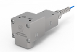 | 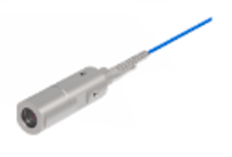 | |
Measurement Type* | Thickness | |
Distance of Use (WD)** | 1.6,10,100 mm | |
Spot diameter | 18~30 ㎛ | |
azimuth resolution | 9~15 ㎛ | |
angle to the surface | 90º ± 2º | |
fiber optic length | 3/4m | |
fiber optic bending angle | 30mm | |
Protective Fiber | Options | |
IP rating | IP68 | IP40 |
Weight cable excluded | 915g | 80g |
Semiconductor
Semiconductor-Wafer Surface Resistance Measurement
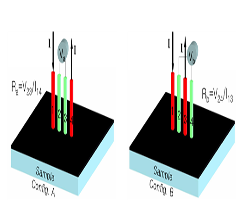
■ Measurement of surface resistance, resistivity
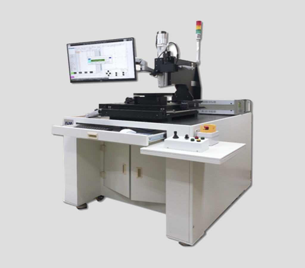
Semiconductor
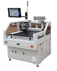
Display
■ Model : AS-SHR, AD-SHR
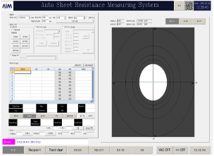
• Measurement of resistance, sheet resistance, resistivity, conductivity<br>
• Save Measurement Data (Date, Sample Model, Custom Selection)
| Model : AS-SHR, AD-SHR | Repeated measurement for each sample after saving custom points | |||
|---|---|---|---|---|
| Vision Aligner Camera | ||||
| Mapping | Wafer : 0~300mm, Display : 1100x1300mm | |||
| measuring range | 1mΩ/sq. ~ 1GΩ/sq. , 10.0 μΩ·㎝ ~ 10.0 MΩ·㎝ | |||
| 2D, 3D Graphic viewer. | ||||
| option | Can be linked to internal processes and instruments by linking SPC and MES | |||
| 응용분야 | Wafer, Display, Thin Film, transistors, diodes, battery electrode materials, solar thin films, organic thin films, MEMS etc. | |||
반도체
반도체-Wafer 평탄도 측정
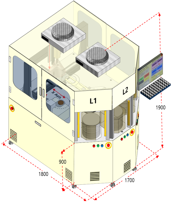
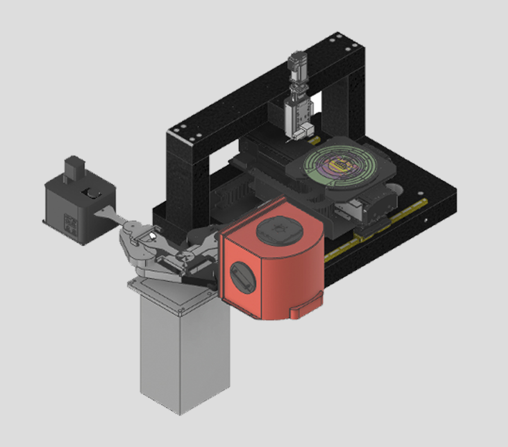
■ 웨이퍼 평탄도 측정기 ( 실리콘 웨이퍼, 사파이어 웨이퍼)
산업용 다관절로봇 사용하여 사파이어 웨이퍼 이송
• 검사 카세트 10개 로딩 가능
• 불량 카세트 4개 로딩 가능
• 1 Cycle Time : ~ 15초 ( 평탄도측정장비 / 측정시간 5초 포함)
– 측정 데이터 실시간 양불 판정 가능
• 측정 화면 스크린샷하여 지정폴더에 저장
• MES 및 SPC 연동 가능


